<< Back to main page

Strained Germanium

Germanium (Ge) is a group IV semiconductor compatible with modern silicon electronics fabrication processes. Ge has an indirect bandgap, so ordinarily it is a poor optical emitter. However, the indirect band-edge is only 0.165 eV below the direct band-edge, and this offset can be decreased or even reversed by applying tensile strain, thus turning Ge into a direct-bandgap material suitable for optical emitters.

Finding suitable fabrication methods to heavily strain Ge while integrating high-Q optical cavities, minimizing non-radiative recombination, and avoiding free carrier absorption can be difficult, but if these obstacles can be overcome, tensile-strained Ge is an excellent candidate for constructing fast and efficient lasers directly alongside conventional silicon electronics.
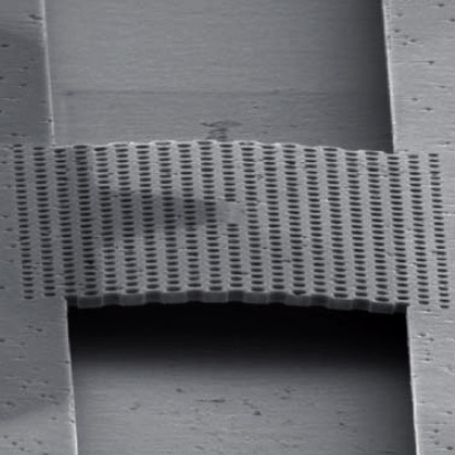
Inverse Design

Today, most electronic logic is designed using hardware description languages like Verilog and VHDL, which are used to specify the circuit's functionality without requiring knowledge of the physical implementation. Meanwhile, most photonic devices are designed by hand, with a designer selecting a design based on intuition and analytic approximations, and then fine-tuning the design with brute-force simulations.

Using a combination of convex optimization techniques and an "objective-first" design approach, in which Maxwell's equations are temporarily violated during the optimization, we have successfully designed and demonstrated a number of state-of-the-art nanophotonic devices. The design process requires no human input beyond the size of the design area, available dielectric materials, and desired functionality.

Ultrafast and Nano-LEDs

In many applications, the modulation rate and energy use of an integrated optical source is more important than its coherence. As a result, nanocavity-coupled light-emitting diodes (LEDs) are excellent candidates as sources for chip-scale optical communications systems, as a high-Q nanocavity can improve the rate of spontanous emission at a single wavelength while suppressing any other emission within a >100 nm spectral window, all while using <1 femtojoule/bit.

Si Nanowire Solar Cells

Silicon (Si) wire arrays offer a solar cell architecture in which the optical absorption path (wire length) can be decoupled from the carrier collection path (radial). This allows them to tolerate lower-purity Si with a short minority carrier diffusion length while retaining the optical absorption characteristics of wafer-based solar cells.

Furthermore, due to optical concentration effects in micron-scale Si wires, Si wire arrays can absorb more light than an equivalent planar volume of Si, even in the ideal ray-optical limit in which both the front and back surfaces of the planar volume scatter light completely randomly.


<< Back to main page